Micro-LED Emission Pattern Microscopy System
MMLEDMSS-NUV-VIS-BP
|
|
|
|
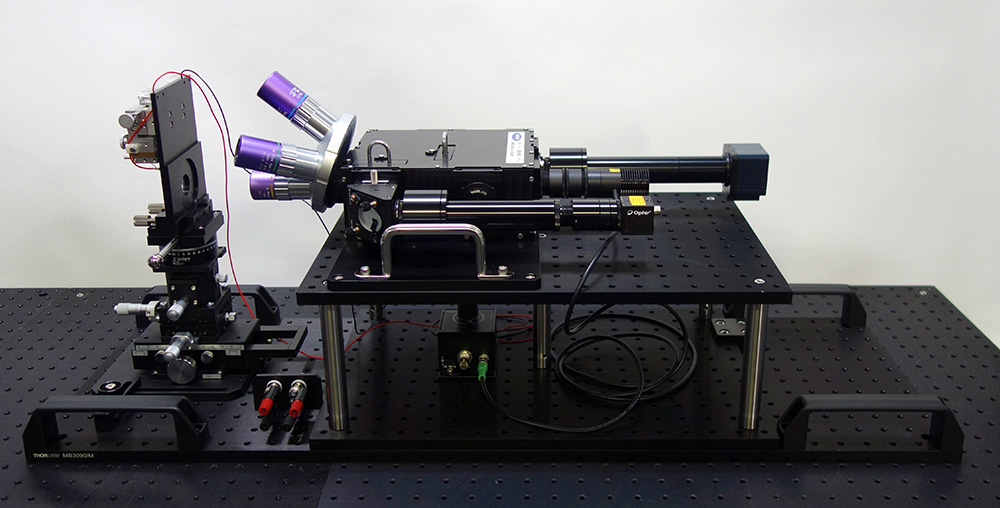
This dedicated system was developed for high-precision observation and measurement of fine emission patterns from micro-LEDs. It combines a compact probe station unit with a high-performance microscope covering the near-ultraviolet to visible wavelength range, enabling detailed observation of emission from both the back and front surfaces of micro-LED devices. The beam profiler measurement unit, included as standard, also enables quantitative measurement and analysis of the optical intensity distribution of emission patterns.
|
■Specifications |
| Probe Station Unit |
| Probe Needles | Material: Tungsten
Tip angle: 5°
Tip radius: 5 μm |
| Manipulators | Total stroke (X, Y, Z): 10 mm per axis
Travel per rotation (X, Y, Z): 250 μm per axis
Number installed: 2 |
| Back-Side Observation Window | Clear aperture: 5 mm diameter |
| X and Y Axes | Travel: ±6.5 mm |
| Z Axis | Travel: ±5 mm |
| Horizontal Slide Axis | Travel: ±50 mm |
|
|
| Microscope Unit |
| Wavelength Range | Aberration-corrected range: 355 nm–620 nm |
| Objective Lens | 10× |
| Revolving Nosepiece | 4 objective positions |
| Filter Ports | 2 ports |
| Optical Input/Output Port | 1 port |
| ND Filters | OD 0.3, 1.0, 2.0, 3.0
AR coating: 350–700 nm |
| Camera | Image sensor: Monochrome CMOS image sensor
Imaging area: 6.41 (H) × 4.59 (V) mm
Pixel size: 1.67 (H) × 1.67 (V) μm
Wavelength range: 400 nm–900 nm
Software: Includes profile measurement functions |
| Illumination | White LED (400–700 nm) coaxial epi-illumination |
|
|
| Beam Profiler Unit |
| Wavelength Range | 190 nm–1100 nm |
| Beam Size | 44 μm–5.3 μm |
| Sensor Type | Silicon CCD |
| Effective Pixel Count | 1624 × 1124 |
| Effective Pixel Size | 4.4 μm |
|
■Measurement Examples |
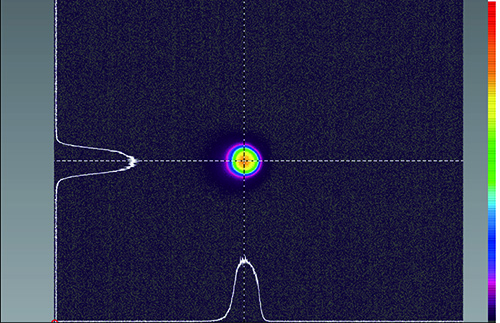
2D
|
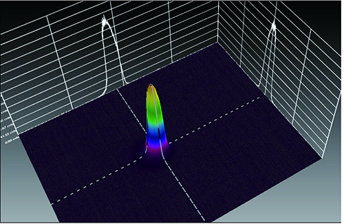
3D
|
Emission spot size: 5 μm
Wavelength: 405 nm
Objective lens: 100×
|
|
| *Specifications and appearance are subject to change without notice for product improvement. |
■About Micro-LEDs |
| A micro-LED (Micro Light Emitting Diode) is a semiconductor device for self-emissive displays and light sources, with individual LED elements miniaturized to micrometer dimensions, typically 10–100 μm. Arranging these extremely small emitters at high density enables high brightness, high contrast, fast response, and long life, offering advantages over conventional liquid crystal and OLED displays. Applications are being developed across a wide range of fields, including next-generation smartwatch and smartphone displays, AR/VR head-mounted displays, large wall displays (digital signage), automotive displays, medical displays, and head-up displays (HUDs). Their fast response and high brightness also make them promising for Li-Fi (visible light communication), optical sensing, and biomedical applications. Micro-LEDs are becoming increasingly important as an enabling technology not only for high-resolution imaging but also for next-generation information display, communication, and sensing. |

