
Wafer-Level LED Test System |
||||||||||||||||||||||||||
 |
||||||||||||||||||||||||||
|
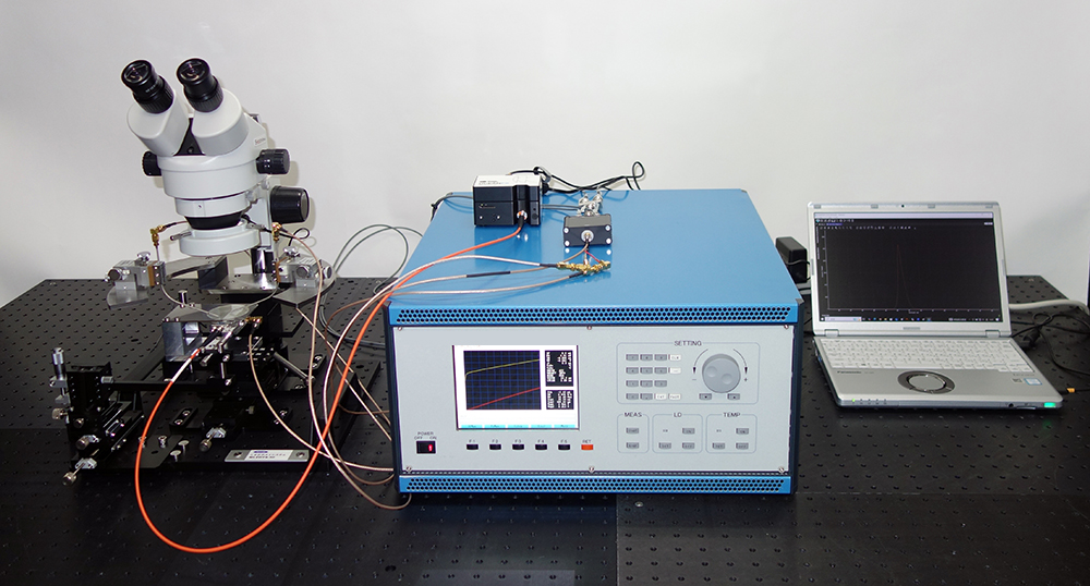
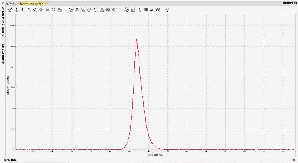
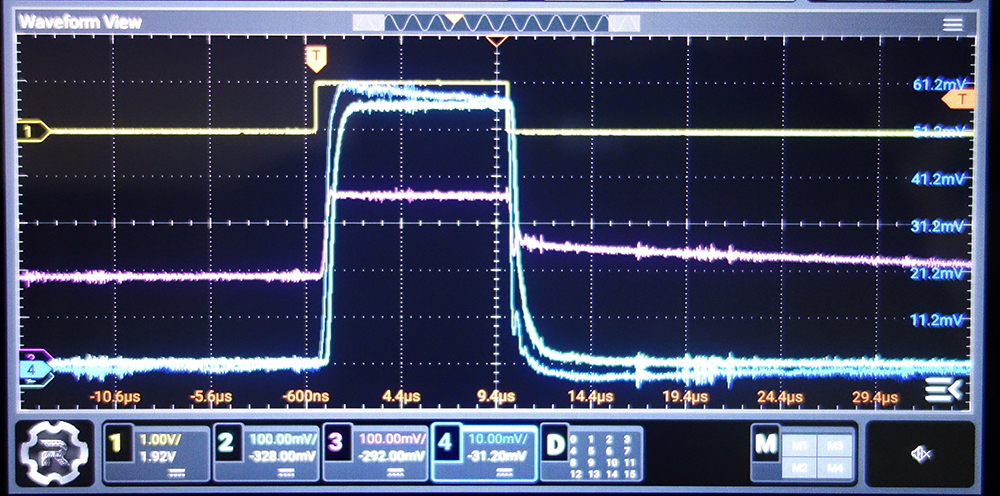
This wafer-level LED test system enables high-precision evaluation of LED chips while they remain on the wafer. It accurately measures electrical and optical parameters, including current–voltage–optical output (I-V-L) characteristics and emission spectra. The system incorporates a pulse driver capable of delivering currents of up to 500 mA with pulse widths as short as 1 μs, enabling characterization with reduced thermal effects on the LED chips. This allows highly reproducible analysis of subtle parameter changes and light-emission efficiency. Wafer-level measurement also offers the significant advantage of evaluating chip characteristics before dicing, helping shorten development cycles and accelerate feedback. Note: The photodiode rise time is 5 μs or longer. |
||||||||||||||||||||||||||
■Specifications |
||||||||||||||||||||||||||
|
||||||||||||||||||||||||||
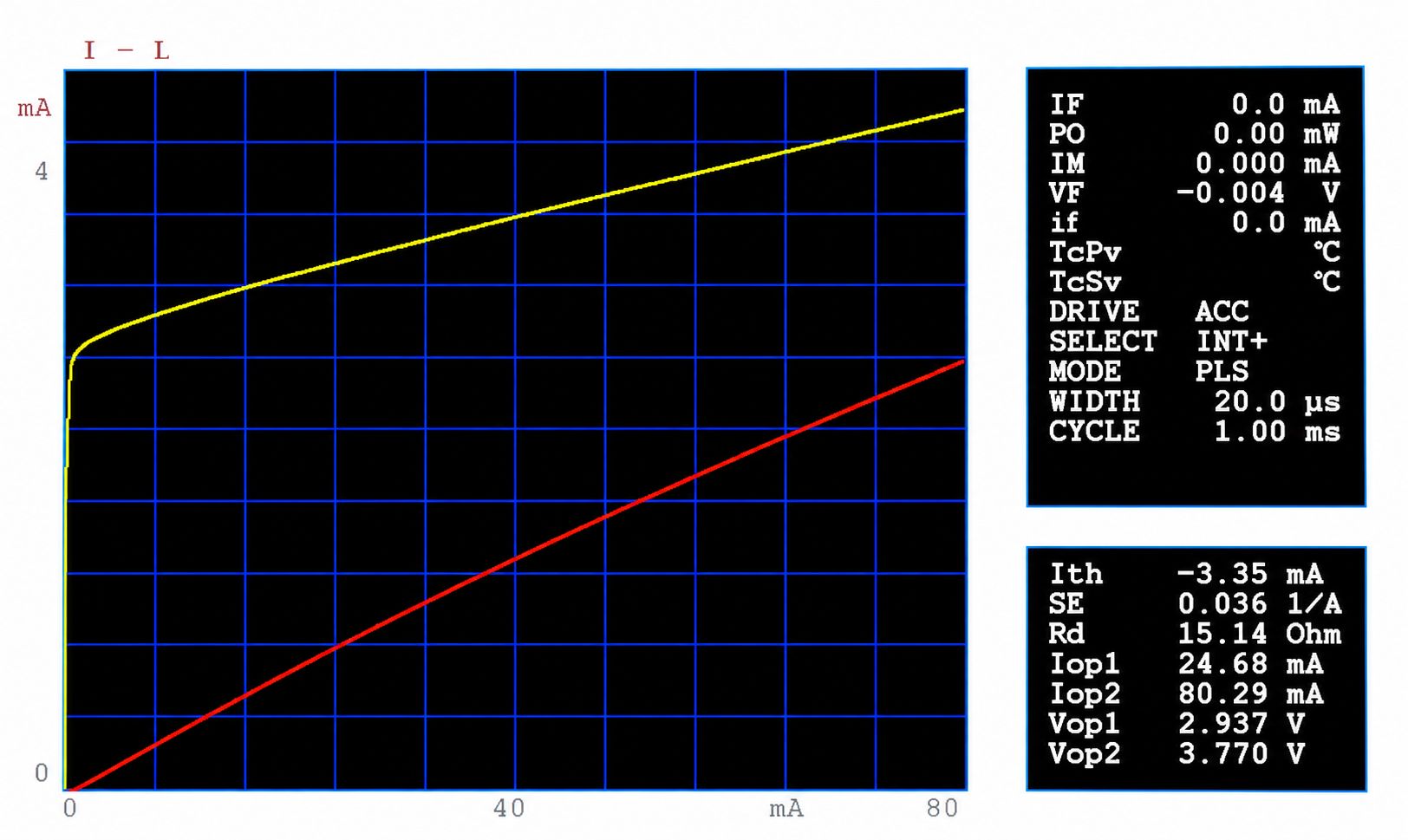
■IVL Characteristic Measurement Data |
||||||||||||||||||||||||||
 |
||||||||||||||||||||||||||
■Emission Spectrum Measurement Data |
||||||||||||||||||||||||||
 |
||||||||||||||||||||||||||
■Pulse Waveforms Measured with an Oscilloscope and Current Probe |
||||||||||||||||||||||||||
 |
||||||||||||||||||||||||||
*Specifications and appearance are subject to change without notice for product improvement. |
||||||||||||||||||||||||||
■About LED IVL Characteristics |
||||||||||||||||||||||||||
| LED IVL characteristics are important indicators for comprehensively evaluating the electrical and optical performance of LED devices. They describe three relationships: current–voltage (I-V), current–optical output (I-L), and voltage–optical output (V-L). I-V characteristics are measured by observing how the current changes as voltage is applied to the LED. They reveal fundamental electrical properties such as turn-on voltage and internal resistance. The characteristic nonlinear diode response, in which current rises sharply above a certain voltage, is used to assess initial device characteristics and identify defective devices. I-L characteristics describe the relationship between the current supplied to an LED and the resulting optical output. They are used to evaluate the onset of optical output, slope efficiency, and light-emission efficiency. These characteristics help determine the optimum drive current and identify optical output saturation or degradation under excessive current. V-L characteristics describe the relationship between voltage and optical output and are generally derived by combining I-V and I-L measurement results. They provide information useful for understanding power efficiency under actual operating conditions, such as mW/W or lm/W, and support energy-efficient design and the selection of operating conditions that reduce heat generation. High-precision measurement and analysis of these IVL characteristics play a vital role in evaluating LED performance, optimizing product development, and supporting quality control and reliability testing. |
