Probe Stations |
| |
| A probe station is a system for wafer-level electrical and optical testing in which probes (needles) are brought into contact with the electrodes of devices fabricated on a wafer, such as ICs, LSIs, LEDs, and laser diodes (LDs). Our probe stations are specifically designed to support optical characterization, enabling wafer-level measurements of light-emitting devices such as LEDs, laser diodes, and VCSELs. The systems comprise a microscope, probing equipment, photodetectors, optical probes, and other components required to perform I-V, I-L, V-L, and spectral measurements. While observing the device through the microscope, the operator brings the probes into contact with the electrodes on the wafer and applies current to characterize the light-emitting device. |
| |
■ Basic Probe Station |
|
|
| |
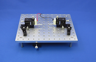
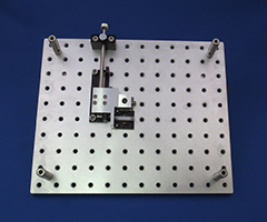
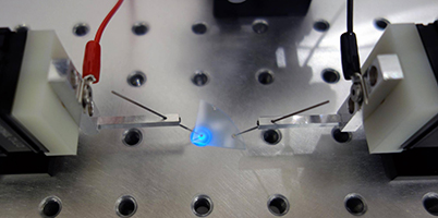
| The basic probe station features a simple structure consisting of probes (needles), manipulators (positioners), and a sample platform. The probes are raised and lowered using the manipulators' Z-axis stages, while alignment with the electrodes is adjusted using their XY-axis stages. Mounts for a photodetector for I-L measurements and an optical fiber for emission spectrum measurements are located on the underside of the probe station plate, allowing the operator to switch between the two measurement configurations. |
| |
■ Manual Probe Station |
| |
|
| |
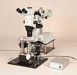
| In the manual probe station, the operator uses manipulators (positioners) to align the probes (needles) with the electrodes of devices on the wafer while observing them through a microscope. The plate supporting the probes and manipulators is then lowered to bring the probes into contact with the electrodes. By raising and lowering the plate and repositioning the wafer between measurements, multiple devices can be measured sequentially. |
| |
■ Semi-Automatic Probe Station |
| |
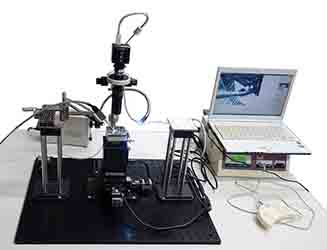
|
| |
| In the semi-automatic probe station, the wafer moves vertically rather than the probe plate. Motorized stages also move the wafer in the XY (horizontal) plane, enabling automatic sequential measurements of multiple devices fabricated on the wafer. First, the operator uses manipulators (positioners) to align the probes (needles) with the device electrodes while observing them through a microscope. The motorized Z-axis stage then raises the wafer to bring the electrodes into contact with the probes for measurement. To move to the next device, the wafer is lowered to separate the electrodes from the probes. The motorized XY-axis stages then position the next device's electrodes beneath the probes, and the motorized Z-axis stage raises the wafer again to establish contact for measurement. Repeating this sequence automatically enables measurements of numerous devices across the wafer. |
| |